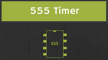
What is a 555 Timer?

Introduction to 555 Timer: The Internal Block Diagram and the Pin Diagram Explained
Catalog

Ⅰ 555 timer design
The 555 Timer is a versatile integrated circuit (IC) widely used in electronic circuits for timing, pulse generation, and oscillation. Designed by Hans R. Camenzind in 1971 for Signetics, the 555 Timer remains popular due to its simplicity, low cost, and reliability (Camenzind, 2007). The 555 timer is designed for Signiitik by Hans R. Camenzind in 1971. Signiitke later was later acquired by Philips. Due to its easy-to-use, low price, and good reliability, it is still widely used in the design of electronic circuits today. Many manufacturers produce 555 chips, including traditional models of bipolar transistors and versions of CMOS design. 555 is considered to be one of the highest-output chips, with about 1 billion yields in 2003.
The 555 Timer integrates 25 transistors, 2 diodes, and 15 resistors within an 8-pin dual in-line package (DIP-8). It is available in various forms, including the NE555 for commercial use and the SE555 for military applications, which operate over a wider temperature range (-55°C to +125°C) (Mims, 2003).
Derivative Models
556: Dual 555 Timer in a 14-pin package.
558/559: Quad timers with additional features.
7555 and TLC555: Low-power CMOS versions.
Different manufacturers have different structures, standard 555 chips integrate 25 transistors, 2 diodes, and 15 resistors, and 8 leads (DIP-8 packages). The derived model of 555 includes 556 (integrated with two 555 DIP-14 chips) and 558 and 559.

555 pin
The NE555 operating temperature range is 0-70 ° C, and the working temperature of the military-grade SE555 is -55 to +125 ° C. The 555 packages are divided into the high-reliability metal package (represented by T) and a low-cost epoxy resin package (represented by V), so 555's full label is NE555V, NE555T, SE555V, and SE555T. The source of the 555 chip name is generally considered to be three 5kΩ resistors, but Hans Camenzind denied this saying and said that the name was randomly selected.
There are also low-power versions, including 7555 and the TLC555. The power consumption of 7555 is lower than the standard 555 timers, and its manufacturer claims that the 7555 control pin is not like a ground capacitor like other 555 chips. And no noise decoupling capacitors are eliminated between the power supply and the ground.
Ⅱ 555 timer pin
The 555 chip of the DIP package is shown in the following table:
Pin | Name | Features |
1 | GND (ground) | Ground, as a low level (0V) |
2 | TRIG(trigger) | When this pin voltage drops to 1 / 3VCC (or the threshold voltage determined by the control), the output is given high. |
3 | OUT | Output high level (+ VCC) or low level. |
4 | RST (reset) | When this pin receives the electricity timer, the chip is reset when this pin is grounded, and the output is low. |
5 | CTRL (control) | The threshold voltage of the chip is controlled. (When the pin is empty, the default two threshold voltage is 1 / 3Vcc and 2 / 3Vcc). |
6 | THR (threshold) | When this pin voltage rises to 2 / 3VCC (or threshold voltage determined by the control), the output is lowered. |
7 | DIS (discharge) | The internal OC gate is used to discharge the capacitor. |
8 | V +, VCC (power) | Provide high levels and power to the chip. |
Ⅲ 555 timer internal structure
The 555 Timer combines analog and digital circuits, featuring a voltage divider, comparators, an R-S flip-flop, and a discharge transistor. The voltage divider consists of three 5kΩ resistors, providing reference voltages for the comparators (Horowitz & Hill, 2015).555 Timer is a mid-scale integrated circuit combined with analog circuit and digital circuit, and its internal structure is as shown below.

555 timer circuit
It consists of a partial part of a voltage divider, a comparator, a substantially R-S flip-flop, and a discharge tripode. The divider is formed by three 5kΩ equivalent resistors. The voltage divider provides the reference voltage to the comparator A1, A2, and the reference voltage of the comparator A1 is applied to the same phase input, and the reference voltage of the comparator A2 is added to the inverting input. The comparator consists of the same integrated op-amp A1, A2 as the two structures. The high-level trigger signal is added to the inverting input of the A1, and after comparing the reference voltage of the same phase input, the result is an input signal of the basic R-S flip-flop terminal; the low-level trigger signal is added to the same phase input of A2. After the reference voltage is compared with the inverting input, the result is an input signal of the basic R-S flip-flop end. The output state of the basic R-S flip-flop is controlled by the output of comparators A1 and A2.
Ⅳ 555 timer uses
The 555 Timer is used in various applications, including:
Monostable Mode: Generates a single pulse of a specific duration.
Astable Mode: Produces continuous square wave signals.
Bistable Mode: Functions as a flip-flop, toggling between two states.
555 timer can work in three working modes:
Single stability mode: In this mode, the 555 function is a single trigger. Applications include timers, pulse loss detection, rebound, tuning switches, divider, capacitance measurement, pulse width modulation (PWM), and the like.
No steady-state mode: In this mode, 555 works in the way in the oscillator. The 555 chip in this working mode is often used in a frequency flash lamp, a pulse generator, a logic circuit clock, a tone generator, a pulse position modulation (PPM). If the thermistor is used as a timing resistor, 555 can constitute a temperature sensor, and the frequency of the output signal is determined by the temperature.
Double steady-state mode (or Schmitt trigger mode): In the case where the DIS pin is vacant and the capacitor is not connected. The 555 work mode is similar to an RS trigger, which can be used to constitute a latching switch.
1.Single stability mode
In the single-stable mode of operation, the 555 timer operates as a single trigger pulse generator. When the input voltage drops to 1/3 of the VCC, the output pulse is output. The output pulse width depends on the time constant of the RC network consisting of the timing resistor and the capacitor. The output pulse stops when the capacitor voltage rises to 2/3 of the VCC. The pulse width can be adjusted by changing the time constant of the RC network based on actual needs.
The output pulse width t, that is, the time required for the capacitance-voltage charges to the VCC, is given by the following formula:
![]()
Although the capacitor is generally considered to discharge the OC gate when the capacitor voltage charges to the VCC, it takes a period of time to discharge, which is called "relaxation time" for a period of time. In practical applications, the cycle of triggering sources must be greater than the sum of relaxation time and pulse width (actually grows much in engineering applications).
2.Double steady mode
555 chip in the dual steady-state mode is similar to the basic RS trigger. In this mode, triggering pin (pin 2) and reset pin (pin 4) pass through the pull-up power to high, the threshold pin (pin 6) is directly grounded, the control pin (pin 5) ground through a small capacitor (0.01 to 0.1 μF), and the discharge pin (pin 7) floating. Therefore, when pin 2 is input high (misleading low) voltage, the output is set, and the reset is output when pin 4 is grounded.
3.No steady mode
The 555 timers can output the square wave of a continuous specific frequency in an uncondensed operating mode. Resistor R1 is connected between VCC and discharge pin (pin 7), and another resistor (R2) is connected between pin 7 and the trigger pin (pin 2), pin 2, and threshold pin (pin 6) short. When the capacitor is charged to 2 / 3VCC through R1 and R2, then the output voltage is flipped, the capacitor is discharged to 1 / 3Vcc by R2, and then the capacitor is recharged, the output voltage is turned again.
For bipolar type 555, if the use of small R1 can cause the OC door to be saturated at the time of discharge so that the low power level time of the output waveform is much larger than the result of the above calculation.
In order to obtain a rectangular wave of less than 50% of the duty cycle, it can be implemented by parallel a diode to R2. This diode is turned on, shorted R2 so that the power supply is only charged only by R1; and when the discharge is turned off to achieve the effect of reducing the charging time to reduce the duty cycle.
Ⅴ 555 timer parameters
The following are the electrical parameters of the NE555, and the 555 timers of other different specifications may have different parameters, please check the datasheet.
Power supply voltage (VCC) | 4.5-16 V |
Rated operating current (VCC = +5 V) | 3-6 mA |
Rated operating current (VCC = +15 V) | 10-15 mA |
Maximum output current | 200 mA |
Maximum power consumption | 600MW |
Minimum working power consumption | 30MW (5V), 225MW (15V) |
Temperature range | 0-70 ° C |
Ⅵ Derivative chip of 555 timer
555 Timers have many different models produced by different companies, with different types of pins, and CMOS design. Some chips include several integrated 555 timers. Some other models of the 555 chip family are as follows:
Mfr | Mfr No | Note |
Avago Technologies | Av-555M | |
Custom Silicon Solutions | CSS555/CSS555C | CMOS, Minimum working voltage 1.2V, IDD<5µA |
CEMI | ULY7855 | |
ECG Philips | ECG955M | |
Exar | XR-555 | |
Fairchild Semiconductor | NE555/KA555 | |
Harris | HA555 | |
IK Semicon | ILC555 | CMOS, Minimum working voltage 2V |
Intersil Corporation | SE555/NE555 | |
Intersil Corporation | ICM7555 | CMOS |
Lithic Systems | LC555 | |
Meixin | ICM7555 | CMOS, Minimum working voltage 2V |
Motorola | MC1455/MC1555 | |
NTE Sylvania | NTE955M | |
RCA | CA555/CA555C | |
STMicroelectronics | NE555N/ K3T647 | |
TI(Texas Instruments) | SN52555/SN72555 | |
TI(Texas Instruments) | TLC555 | CMOS, Minimum working voltage2V |
Zetex | ZSCT1555 | Minimum working voltage 0.9V |
NXP | ICM7555 | CMOS |
HFO | B555 | |
HITACHI | HA17555 |
Conclusion
The 555 Timer's enduring popularity is a testament to its versatility and reliability. Its ability to function in multiple modes makes it an essential component in both educational and professional electronic projects.
References
Camenzind, H. R. (2007). Designing Analog Chips. Lulu.com.
Horowitz, P., & Hill, W. (2015). The Art of Electronics (3rd ed.). Cambridge University Press.
Mims, F. M. (2003). Getting Started in Electronics. Master Publishing, Inc.
1.What does a 555 timer do?
The 555 timer IC is a very cheap, popular, and useful precision timing device that can act as either a simple timer to generate single pulses or long time delays or as a relaxation oscillator producing a string of stabilized waveforms of varying duty cycles from 50 to 100%.
2.How fast can a 555 timer go?
TI's LMC555 claims to be the smallest and fastest fully-featured 555 available. This is a CMOS variant, with a maximum frequency of 3 MHz according to the datasheet. It's available in a variety of 8-pin packages, including DIP, SOIC, and VSSSOP, in order of decreasing size.
3.How do you use a 555 timer?
An Astable Multivibrator can be produced by adding resistors and a capacitor to the basic timer IC 555. The timing during which the output is either high or low is determined by the externally connected two resistors and a capacitor. Clock: A clock is simply a square wave i.e. alternate high & low states.
4.How do you trigger a 555 timer?
Usually, the timer IC 555 is triggered by applying a negative-going pulse to its trigger pin 2. This timer is triggered through a positive pulse in its reset pin. In the monostable mode, IC 555 starts the timing cycle when a negative pulse is applied to its trigger pin 2.
5.How accurate is a 555 timer?
For less than 1% accuracy, the 555 timer is an ideal choice. For an accuracy better than 0.1%, consider digital or crystal techniques. Occasionally the 555 will suffer from jitter problems on its output if the supply- voltage variations are rapid with respect to the timing cycle.
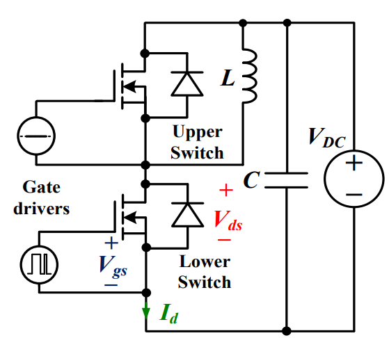
 Discovering New and Advanced Methodology for Determining the Dynamic Characterization of Wide Bandgap DevicesSaumitra Jagdale15 March 20242497
For a long era, silicon has stood out as the primary material for fabricating electronic devices due to its affordability, moderate efficiency, and performance capabilities. Despite its widespread use, silicon faces several limitations that render it unsuitable for applications involving high power and elevated temperatures. As technological advancements continue and the industry demands enhanced efficiency from devices, these limitations become increasingly vivid. In the quest for electronic devices that are more potent, efficient, and compact, wide bandgap materials are emerging as a dominant player. Their superiority over silicon in crucial aspects such as efficiency, higher junction temperatures, power density, thinner drift regions, and faster switching speeds positions them as the preferred materials for the future of power electronics.
Read More A Comprehensive Guide to FPGA Development BoardsUTMEL11 September 202515542
This comprehensive guide will take you on a journey through the fascinating world of FPGA development boards. We’ll explore what they are, how they differ from microcontrollers, and most importantly, how to choose the perfect board for your needs. Whether you’re a seasoned engineer or a curious hobbyist, prepare to unlock new possibilities in hardware design and accelerate your projects. We’ll cover everything from budget-friendly options to specialized boards for image processing, delve into popular learning paths, and even provide insights into essential software like Vivado. By the end of this article, you’ll have a clear roadmap to navigate the FPGA landscape and make informed decisions for your next groundbreaking endeavor.
Read More Applications of FPGAs in Artificial Intelligence: A Comprehensive GuideUTMEL29 August 20253794
This comprehensive guide explores FPGAs as powerful AI accelerators that offer distinct advantages over traditional GPUs and CPUs. FPGAs provide reconfigurable hardware that can be customized for specific AI workloads, delivering superior energy efficiency, ultra-low latency, and deterministic performance—particularly valuable for edge AI applications. While GPUs excel at parallel processing for training, FPGAs shine in inference tasks through their adaptability and power optimization. The document covers practical implementation challenges, including development complexity and resource constraints, while highlighting solutions like High-Level Synthesis tools and vendor-specific AI development suites from Intel and AMD/Xilinx. Real-world applications span telecommunications, healthcare, autonomous vehicles, and financial services, demonstrating FPGAs' versatility in mission-critical systems requiring real-time processing and minimal power consumption.
Read More 800G Optical Transceivers: The Guide for AI Data CentersUTMEL24 December 20254450
The complete guide to 800G Optical Transceiver standards (QSFP-DD vs. OSFP). Overcome supply shortages and scale your AI data center with Utmel Electronic.
Read More Xilinx FPGAs: From Getting Started to Advanced Application DevelopmentUTMEL09 September 20254406
This guide is your comprehensive roadmap to understanding and mastering the world of Xilinx FPGA technology. From selecting your first board to deploying advanced AI applications, we'll cover everything you need to know to unlock the potential of these remarkable devices. The global FPGA market is on a significant growth trajectory, expected to expand from USD 8.37 billion in 2025 to USD 17.53 billion by 2035. This surge is fueled by the relentless demand for high-performance, adaptable computing in everything from 5G networks and data centers to autonomous vehicles and the Internet of Things (IoT). This guide will walk you through the key concepts, tools, and products in the Xilinx ecosystem, ensuring you're well-equipped to be a part of this technological revolution.
Read More
Subscribe to Utmel !
![SI8261ACC-C-IS]() SI8261ACC-C-IS
SI8261ACC-C-ISSilicon Labs
![HCS301T/SN]() HCS301T/SN
HCS301T/SNMicrochip Technology
![ADUM3224WCRZ]() ADUM3224WCRZ
ADUM3224WCRZAnalog Devices Inc.
![SI8233AD-D-IS]() SI8233AD-D-IS
SI8233AD-D-ISSilicon Labs
![ATECC508A-MAHCZ-S]() ATECC508A-MAHCZ-S
ATECC508A-MAHCZ-SMicrochip Technology
![ATECC608A-SSHCZ-B]() ATECC608A-SSHCZ-B
ATECC608A-SSHCZ-BMicrochip Technology
![AT88SC0808CA-MJ]() AT88SC0808CA-MJ
AT88SC0808CA-MJMicrochip Technology
![HCS361-I/P]() HCS361-I/P
HCS361-I/PMicrochip Technology
![ACPL-J313-500E]() ACPL-J313-500E
ACPL-J313-500EBroadcom Limited
![ADUM7234BRZ-RL7]() ADUM7234BRZ-RL7
ADUM7234BRZ-RL7Analog Devices Inc.


 Product
 Brand
Brand Articles
 Tools
Tools


